

Technology
Innovation
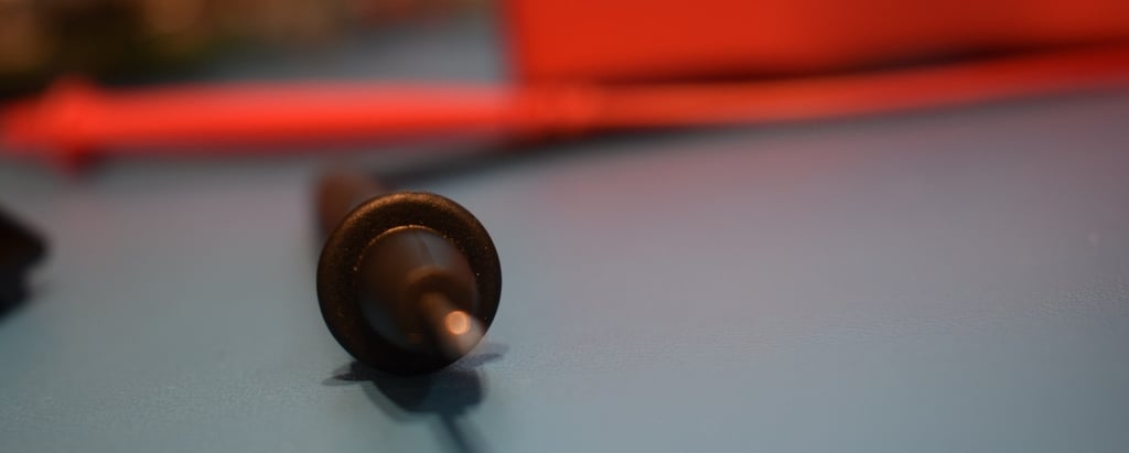
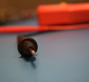
The race to eliminate historical MOSFET devices for a higher performing technology is achieved with lateral GaN HEMT market offerings. GaN HEMT technology provides an extreme advantage of highest power switching speeds. Various commercial supply offer GaN HEMT devices ranging from low voltage (40V) up and through 650V commercial technology. Unlike these companies, Semi-Zabala's GaN processing and it's specific designs are developed to survive radiation effect environments. Semi-Zabala's innovations realized the highest voltage radiation survivability of any industry supplied lateral GaN HEMT device sustaining 600V+ ratings without degradation in space borne heavy ion testing environments, fully validated up to 83MeV Au levels.
Primary Focus
Design initially, then manufacturing (initially without being a qualified facility then with full qualification for space components etc..) then qualification (screening, burn-in etc…)

THE APPLICATION OF GAN TECHNOLOGY
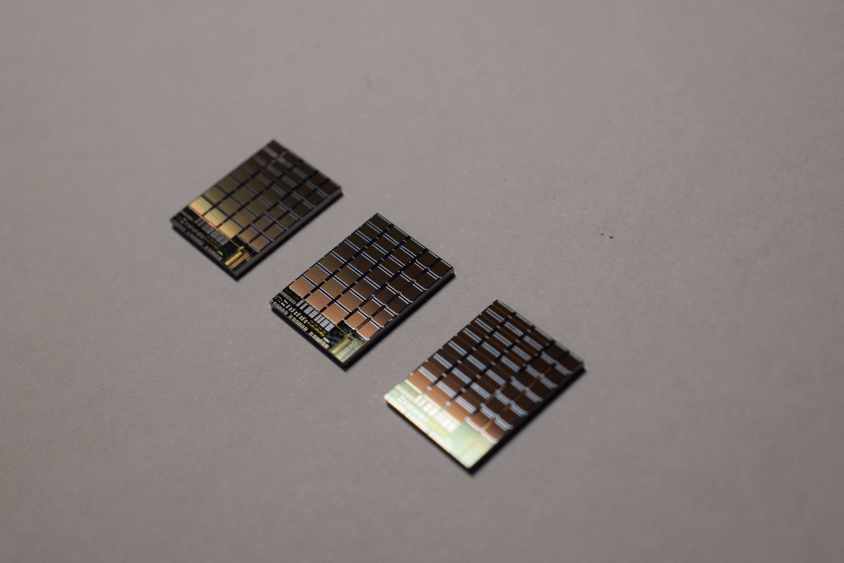
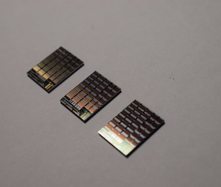
Gallium Nitride (GaN) and particularly enhancement mode high electron mobility transistors (HEMT E-Mode GaN) are WBG semiconductors offering significant advancements to the power electronics world. Silicon(SI) technology has been the historical workhorse of industry with typical bandgap of 1.1eV. Some of the key WBG materials actively being adopted while providing proven stability are both silicon carbide (SiC) and gallium nitride (GaN), these advanced technologies possess significantly greater bandgaps of 3.3 eV and 3.4 eV respectively with other additional significant attributes. Semi-Zabala is dedicated to advancing HEMT GaN material designs at highest breakdown voltage, higher thermal conductivity and greater efficiencies, coupled to a significant radiation resistance far superior to historical Si Rad Hard Mosfets.
Critical path system platforms such as defense, commercial space, and high-end industrial have sought technologies surpassing current Si based power capabilities particularly those offering higher power density at a lower cost, smaller size, greater overall efficiencies while maintaining reliability demands for critical path systems. Semi-Zabala offers such capabilities with extreme radiation design performance of full single effects survival paired to the highest breakdown voltages of any in the market today. Our Radiation Hardened design platforms specifically offer technology advancements ratings at 100V, 200v, 400V up to +600V breakdown voltages.
Semi Zabala
Leading the way in semiconductor technology solutions.
Contact
Newsletter
info@semizabala.com
+34 647 910 665
© 2026. All rights reserved.
Terms & Conditions


Head offices: Avenida de la Libertad 25-7, Donostia-San Sebastián 20004
Production location: Txaldatxur 4, Zubieta, Donostia-San Sebastián 20160